AI · 19 November 2026 · 4 min read
ASE Breaks Ground on NT$248.9 Billion ($7.6B) AI Semiconductor Testing Hub in Kaohsiung
Paired with neighboring K Block, ASE’s Renwu Industrial Park testing complex reaches $11.1 billion in planned capital deployment ahead of phased 2028–2029 completion.
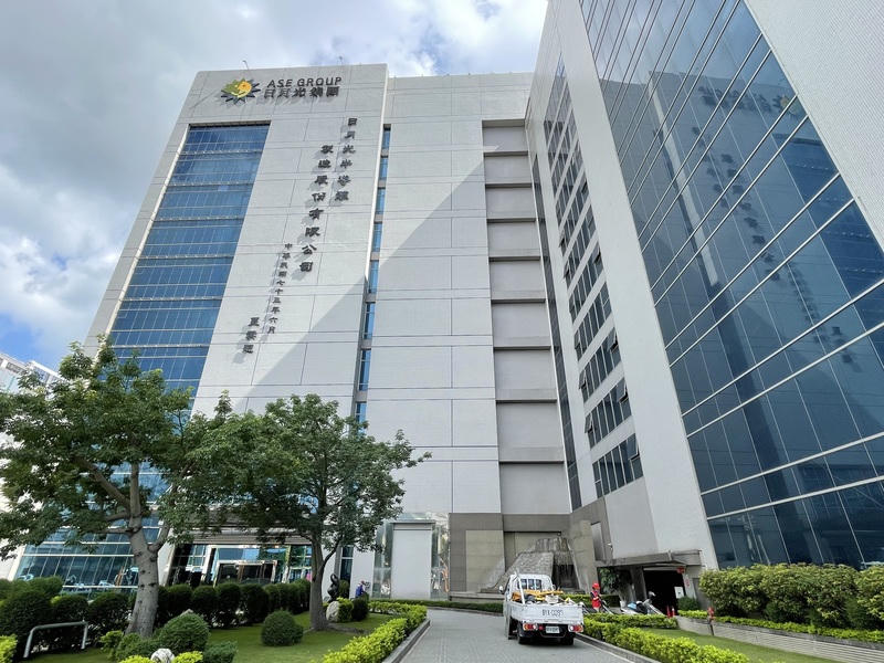
ASE Technology Holding Co. (NYSE: ASX), the world’s largest outsourced semiconductor assembly and test (OSAT) provider, broke ground on November 19, 2026, on a NT$248.9 billion (approximately $7.6 billion) AI chip testing facility in Kaohsiung’s Renwu Industrial Park (MLQ.ai; BigGo Finance, Nov. 19, 2026).
Marking ASE’s second major Kaohsiung commitment in less than a week, the groundbreaking highlights an evolving supply-chain bottleneck: as multi-chiplet AI accelerators grow denser and more power-hungry, post-fabrication burn-in, thermal validation, and advanced packaging have become as capacity-constrained as leading-edge wafer fabrication.
Technical & Financial Breakdown
Built through subsidiary Taiwan Foredge Electronics, the new J Block facility is roughly 2.1 times the size of the NT$117.45 billion (~$3.6 billion) investment ASE committed to adjacent K Block in April 2026 (BigGo Finance, Nov. 19, 2026). Combined planned investment across both Renwu blocks now stands at NT$366.35 billion (~$11.1 billion).
ASE targets phased construction completion across 2028 and 2029, projecting NT$117.3 billion (~$3.6 billion) in combined annual revenue and 3,300 jobs at full scale. Chief Executive Officer Tien Wu stated at the ceremony that Renwu will serve as ASE’s largest testing complex, engineered for peak automation density and revenue per employee.
The project follows ASE’s November 13 inauguration of Phase 1 and groundbreaking of Phase 2 at its NT$100 billion (~$3.05 billion) Luzhu advanced packaging site in the Southern Taiwan Science Park (Taipei Times, Nov. 13, 2026). Last month, ASE raised its full-year 2026 capital expenditure (CapEx) budget for the third time to $11.5 billion to meet leading-edge AI demand.
Second-Order Implications
For US silicon designers—including NVIDIA, AMD, Broadcom, and hyperscaler custom-ASIC teams—ASE’s multi-billion-dollar buildout confirms that test times per AI package are climbing sharply. High-power rack-scale accelerators like Vera Rubin NVL72 require far longer thermal stress testing and high-speed interconnect validation before final system integration.
For semiconductor capital equipment investors, ASE’s $11.5 billion annual CapEx pace signals multi-year demand visibility for automated test equipment (ATE), probe-card manufacturers, and automated material-handling vendors.
Caveats & Open Questions
The NT$248.9 billion figure reflects a multi-year planned investment announced at groundbreaking rather than locked-in customer purchase orders, and meaningful J Block capacity will not come online until 2028–2029. Placing another $11.1 billion of critical AI testing infrastructure in southern Taiwan also intensifies geographic supply-chain concentration risk for US hyperscalers already heavily exposed to Taiwan’s semiconductor ecosystem.
More in AI